



Why Flat Chips Are Running Out of Road
For decades, the semiconductor industry followed a reliable rhythm: shrink the transistors, pack more onto a flat silicon wafer, and watch performance climb. This principle, loosely captured by Moore’s Law, drove everything from personal computers to smartphones. But that rhythm is faltering. Transistors are now so small — measured in just a few nanometers — that fundamental physical limits are beginning to interfere. Electrons leak, heat builds up, and the cost of each new fabrication node has skyrocketed.
Engineers and researchers have been asking a straightforward question: if we can’t keep going sideways, why not go up? The answer has given rise to one of the most promising directions in modern chip design — 3D chip stacking.
What Vertical Integration Actually Means in Silicon
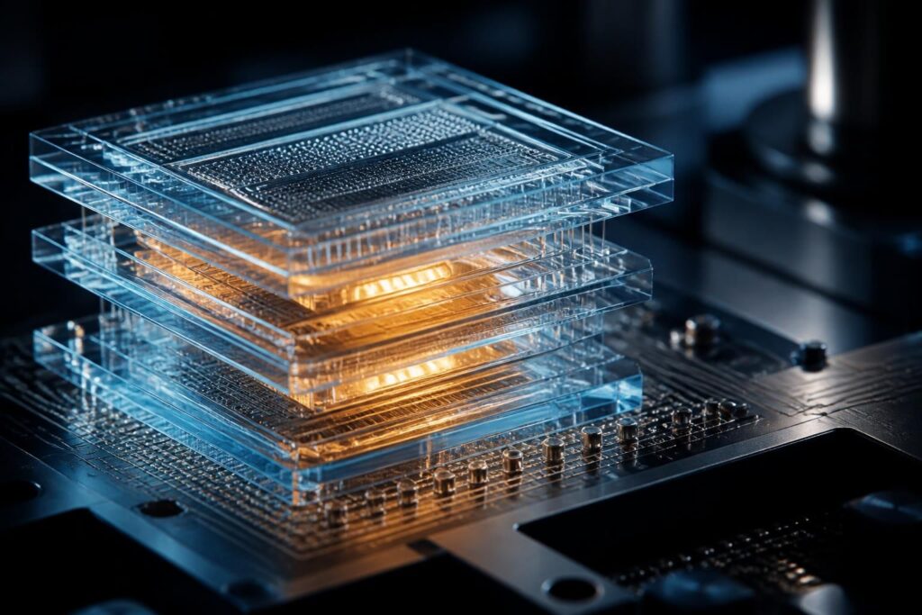
The concept is intuitive, even if the engineering is anything but. Instead of placing all components on a single flat die, manufacturers layer multiple chips — or chiplets — directly on top of one another, connecting them through incredibly dense vertical pathways known as Through-Silicon Vias (TSVs). These microscopic tunnels allow data and power to travel between layers at speeds and densities that traditional side-by-side wiring simply cannot match.
Think of it like the difference between a sprawling single-story warehouse and a tightly packed skyscraper. The skyscraper fits far more into the same footprint, and crucially, the distances between floors are much shorter than the distances across a wide floor plan. In chip terms, shorter distances mean lower latency and less energy consumed per operation.
“The interconnect bottleneck is the real enemy of performance today. Stacking chips is not just a packaging trick — it’s a fundamental rethinking of how we move data inside a computer.” — Dr. H.S. Philip Wong, Stanford University
The Technologies Driving the Stack
Several distinct approaches are emerging, each suited to different use cases:
- 2.5D integration: Chips sit side by side on a shared interposer substrate, offering improved communication without full vertical stacking. AMD’s EPYC processors and their HBM memory configurations use this approach.
- 3D stacking with TSVs: True vertical layering with direct electrical connections through the silicon itself. HBM (High Bandwidth Memory) is the most commercially mature example, widely used in AI accelerators and high-performance GPUs.
- Monolithic 3D integration: The most ambitious approach, where transistor layers are built directly on top of each other during fabrication, rather than bonded afterward. This promises the densest connections but remains largely in the research phase.
- Hybrid bonding: A newer technique that fuses two chip surfaces together at the atomic level, enabling connection pitches below one micrometer — far tighter than traditional solder bumps allow.
Companies like TSMC, Intel, and Samsung are all investing heavily in these techniques. Intel’s Foveros technology, for instance, allows logic chips to be stacked directly on top of one another, enabling products like the Meteor Lake processor family that blend different chip types from potentially different manufacturers.
Why This Matters Beyond Raw Speed
Performance gains are the obvious headline, but the implications run deeper. One of the most significant benefits of 3D stacking is energy efficiency. Moving data across long, flat interconnects consumes a disproportionate amount of power in modern chips. By shortening those pathways dramatically, stacked architectures can deliver the same computational throughput at a fraction of the energy cost — a critical consideration as data centers consume an ever-growing share of global electricity.
There’s also the question of chiplet modularity. Rather than designing one enormous monolithic chip — which becomes increasingly expensive and prone to manufacturing defects as it grows larger — engineers can now combine smaller, specialized dies. A processor might stack a high-performance compute core made on a cutting-edge node with a memory layer or I/O chip made on a cheaper, older node. This mix-and-match approach can significantly reduce costs while improving yields.
For artificial intelligence workloads in particular, the ability to place memory physically adjacent to compute logic is transformative. The so-called memory wall — the growing gap between how fast processors can compute and how quickly they can access data — is one of the central bottlenecks in modern AI training and inference. Stacked memory directly addresses this problem.
Challenges That Still Need Solving
The path forward is not without serious obstacles. Heat dissipation is arguably the most pressing concern. When chips are layered on top of each other, the lower layers have no direct path to cooling solutions mounted on the top surface. Engineers are exploring liquid cooling channels embedded within the silicon stack itself, but this adds complexity and cost.
Testing is another headache. With conventional flat chips, each die can be tested before assembly. In a tightly bonded stack, a defect in one layer can compromise the entire assembly — a costly outcome when individual layers may contain billions of transistors. Known Good Die (KGD) testing protocols are improving, but the challenge remains significant.
Standardization is also lagging behind innovation. For the chiplet ecosystem to truly flourish, different manufacturers need to agree on common interfaces. The Universal Chiplet Interconnect Express (UCIe) standard, backed by a broad industry consortium, is a promising step in this direction, but widespread adoption will take time.
A Glimpse at What’s Coming
Despite these hurdles, the trajectory is clear. Research institutions and major chipmakers are already demonstrating prototype stacks with four, six, and even more active layers. The combination of 3D stacking with other innovations — such as photonic interconnects and new materials like gallium nitride — could push computing performance well beyond what silicon scaling alone could ever achieve.
The skyscraper analogy holds up remarkably well. Just as cities built upward when horizontal land ran out, the chip industry is discovering that the next frontier of performance lies not on the surface of silicon, but within its depths. The revolution may be quiet and largely invisible to end users, but its effects — faster AI, more efficient data centers, longer battery life in mobile devices — will be anything but.